[Home] [ROM] [Static RAM] [Dynamic RAM] [Synch. RAM] [FGPA Mem.] [FIFO buffers] [ Up ] [ ROM Based Statemachines ]
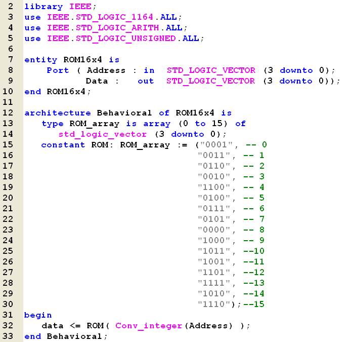
This ROM created for the purpose as "next state" logic. Exercise: Connect the Data (output) with the Address (input) through 4-D-F/F. Which pattern can be observed at the 4 Data bits.
This ROM created for the purpose as "next state" logic.
Exercise:
Connect the Data (output) with the Address (input) through 4-D-F/F.
Which pattern can be observed at the 4 Data bits.
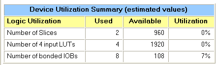
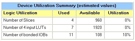
Notice! the optimal usage of FPGA resources.4 LUTs = 16x4bit
4 LUTs = 16x4bit
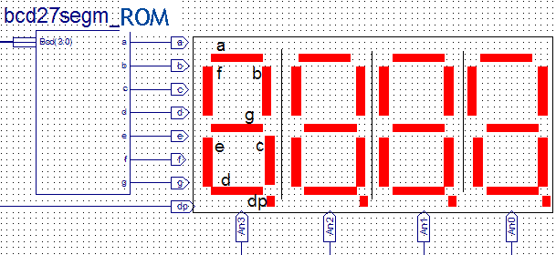
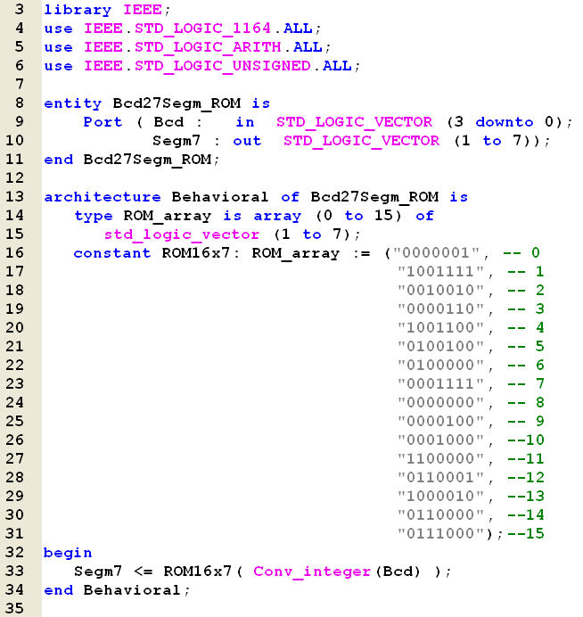
The Bcd27Segm driver also an subject for implementation as a ROM (16x7bit)
Notice! the optimal usage of FPGA resources.7 LUTs = 16x7bit
7 LUTs = 16x7bit
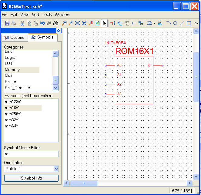
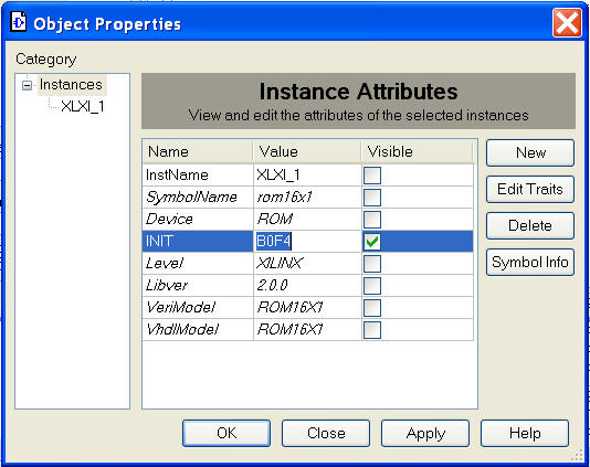
ROM blocks can also be defined directly with a Schematic SymbolThe content defined with the INIT Attribute
The content defined with the INIT Attribute
The content defined with the INIT Attribute Here set to B0F4(hex) and made Visible.
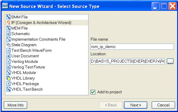
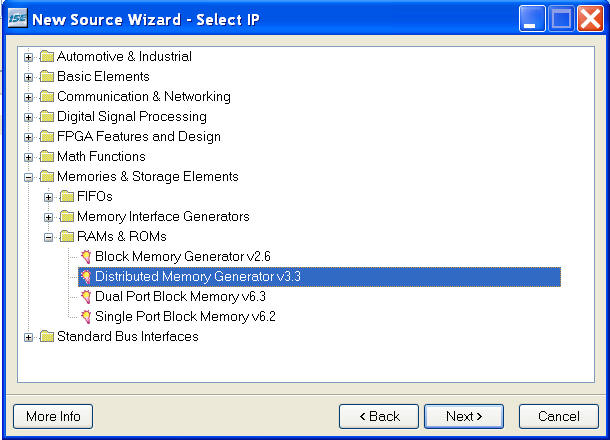
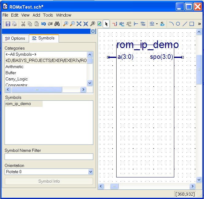
Alternative way of ROM definition - an IP core
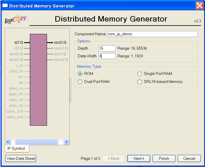
The Distributed Memory Generator will use LUTs as ROM/RAM
Depth and Data Width
The Automatic generated Schematic Symbol